Select language Select language Select language
 Obtain high-resolution images of selected areas to identify the causes of failure
Discover the service
Discover the service
Scanning electron microscopy, also known as SEM analysis, is the main technique used to investigate the causes of failure in failure analysis and allows morphological investigations of surfaces to be carried out with magnifications of up to 400,000x. Thanks to these images, it is possible to analyse, for example, ductile and brittle fracture zones, beach lines, contaminants, hydrogen embrittlement and corrosion.
For scanning electron microscopy analysis, we chose to use a SEM microscope with Zeiss technology, while for EDS/EDX microprobe analysis, which provides important chemical information on specific points or selected areas, we chose Oxford technology.
Pontlab is accredited as test laboratory No. 1286 L by Accredia.
Metallic Materials
Advanced Materials
Automotive
Aerospace
Industrial
Electronics
We perform a variety of scanning electron microscopy tests, both standardised and customised, to obtain high-resolution images and identify the causes of failure.
Request a consultation
This test allows the surface structure of materials to be observed in high resolution, analysing defects, fractures, wear and contamination on a micrometric and nanometric scale.
It is used in sectors such as metallurgy, electronics, automotive and cultural heritage for the study of metallic, polymeric and composite materials. The analysis provides information on roughness, porosity and defect distribution.

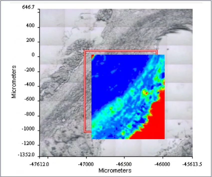
Combined with SEM microscopy, EDS spectroscopy allows the chemical elements present in a sample to be identified and quantified. This technique is used to check for contamination, non-metallic inclusions and compositional variations in materials such as metal alloys, ceramics and polymers, and is widely used in the manufacturing industry and failure analysis.

This technique is fundamental for analysing material failure mechanisms. It allows the causes of fracture (brittle, ductile, fatigue or corrosion) to be identified by observing the fracture surfaces. It is used in the aerospace, automotive and industrial sectors to improve design and prevent premature failure.

This test allows the quality of surface treatments, such as protective coatings, plating and oxidation, to be studied by checking the adhesion, thickness and uniformity of the deposited layer.
It is used in sectors such as biomedicine, electronics and materials engineering to ensure compliance with technical standards.

Using SEM in high-resolution mode, it is possible to examine the morphology and distribution of nanoparticles in materials. This technique is essential in the pharmaceutical and environmental fields and in new advanced materials for quality control and research on nanostructures.


All analyses can be structured in a completely customised manner, based on customer requirements. We offer tailor-made tests for materials, conditions of use and required regulations, ensuring reliable and targeted results.
For further insights, articles, and regulations on material corrosion, visit the CORROSIONPEDIA portal (https://www.corrosionpedia.com)
Visit the website
The SEM electron microscope enables high-resolution analysis of surfaces and microstructures, supporting sectors such as electronics, aerospace and cultural heritage in research and quality control.
All tests can be performed in a completely customized manner, adapting to the customer's needs. Pontlab also offers tailored consulting services to define the most suitable tests, ensuring reliable and targeted results.
In addition to scanning microscopy tests, Pontlab performs countless other tests, including on different materials such as polymers, fabrics, leather and paints. Discover the other tests by visiting the dedicated pages.